|
||||||||||||||||||

|
Analog Board Build Introduction
When I ordered my DAC Kit 2.1, I was told that there would be two options available for the analog board itself. If I was willing to wait, there would be a normal printed circuit board available - or I could have a silver hard-wired one now.
Personally, I will always go for a silver hard-wired version of any board if available so that is the one shown here.
I would imagine that the printed circuit version would be a very simple board to build, as there are not many components on this particular board so it shouldn't be too much of an omission here for those of you who have decided to go for the PCB version.
Unlike the Kit1 Phono Stage that I built previously, the analog hard-wired board here was one that is used in other kits and, as such, wasn't marked up for this project. This meant that the markings that show component placement (on the top) and interconnections (on the rear) were not valid for this project.
In fact, the manual gets you started on the connections but it is mainly up to you how the components are connected - you simply follow the circuit diagram and make the appropriate connections. That made me decide to put more detail into this section than usual in order to help and encourage people who have decided to go for the hard-wired option.
|
|
|
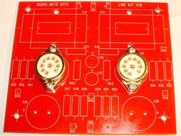
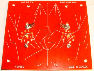
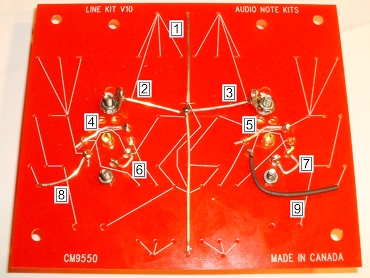
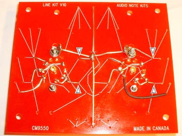
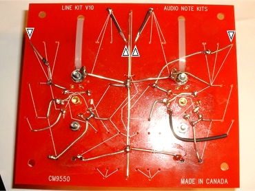
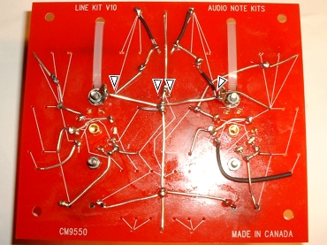
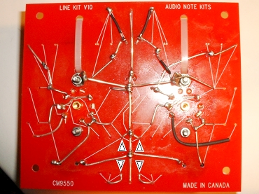
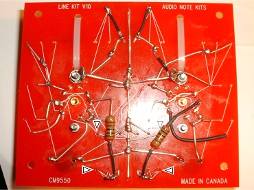
This is the silver hard-wired version of the analog board (a printed circuit board version is also available). There are no tracks like you would find on a normal printed circuit board. The markings that you see on the reverse of the board are usually an aid to the hard-wiring but, because the board comes from a different kit, they are not valid for this project.
You have to make all the connections yourself. You do this in one of three ways:
- Using component legs
- Using the supplied silver wire
- Extending component legs with silver wire
To get maximum connection via surface area, wires should be wrapped around other wires before soldering.
This method will always yield superior results to a printed circuit board because rather than there being a very thin layer of copper track providing conductivity, there is instead a significant mass of silver or the uninterrupted tinned copper leads of components. Also, there is better surface area contact than with PCB's which can be important.
To get the best out of the process it is also advisable to use silver solder (as I always do with my audio projects anyway).
I began planning the component placing and wiring by using the photographs of each side of the board and putting them in a drawing package, side-by-side. For each stage, I made a copy of them, changed all the previous connection lines to gray, and drew the next set of connections. I then followed the drawings sequence to make the actual connections etc. that were then photographed and shown below.
Before You Start
I have deviated form the way shown in the manual and have done it my way (which is what you're supposed to do really). Besides, the manual simply shows you how to get started and gives you the basic tips that you need to proceed.At each step of the way, you should mark off your progress on a copy of the circuit diagram - I find it useful to use a highlighting pen to do this. Then, once the diagram has been fully marked out, you know that the board is ready.
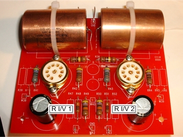
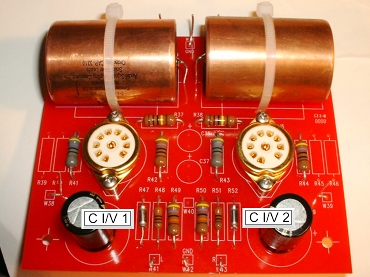
The Level B version of the analog board build is different from a Level A build. The Level B version has two extra components per channel that are necessary to couple the I/V transformers. Therefore, I decided to leave those components until the very last so that this page would also be useful to Level A builders.
Bear in mind that the way I have built this board is not necessarily the 'best' way to do it and you may come up with a completely different way of doing it. The important thing is that all connections are correctly made and there should be no danger of shorting.
The thing that is not easy to show is the 3D nature of the wiring. Although wires may appear to be crossing and making contact in the pictures they probably aren't unless you can see a significant 'lump' where a join would be.
Fitting the Valve Bases
Our first job is to fit the valve bases onto the board.
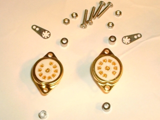
Above are the fittings for the valve bases. They use spacers to lift them away from the board's surface and are held in place with screws and nuts. We will also use a ground lug at one end of each valve base; on the underside of the board.
|
|
|
As you can see, I decided to put the ground lugs at the 'top'. These will, however, need to be bent further upward because some component legs will come quite close to them later.
|
|
Initial Wiring
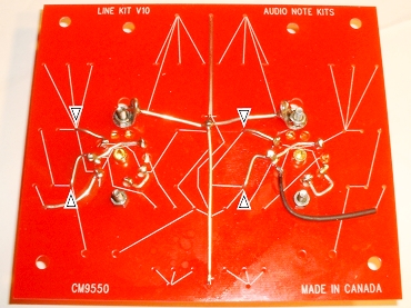
Before inserting my first components, I took care of some wire connections. The most important is the central ground bus.
|
|
||||||||||||
|
|||||||||||||
Adding the Components
I will be showing one picture per component stereo pair. In other words, the same component from each channel will be inserted and a picture of the front and back of the board shown. The arrows point to the holes where the components pass through the board.
|
|
|
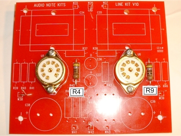
The first components to be added are R4 and R9. One end connects to pin 2 of the valve base (which can now be soldered). The other end connects to pin 3.
|
|
|
|
|
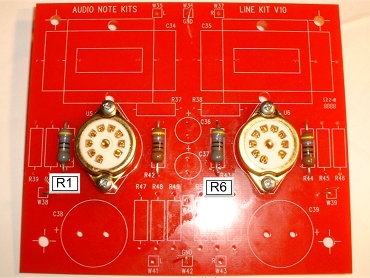
Next are R1 and R6. One end connects to ground and the other connects to the loop we made between pins 8 and 9.
|
|
|
|
|
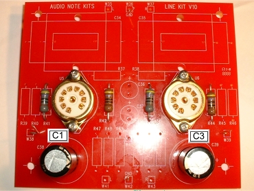
Now the electrolytics C1 and C3. These must be inserted the correct way around. Here the board markings in that position are valid in their markings for + and - positions. The negative leg goes to ground and the positive leg connects to the loop we made at pins 8 and 9.
|
|
|
|
|
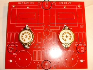
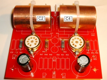
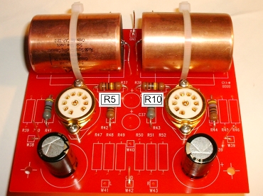
The coupling capacitors C2 and C4 are very large and require that they are secured to the board with tie-wraps. One end, the one closest to the centre (in both cases), is fed through the board to create the terminals W35 and W37. There is actually no need to insulate these as I have done. However, it must be noted that they are very close to the ground bus and must not be allowed to touch it! The other end is connected to the leg of R4/R9. The leads are not long enough on their own and need to be extended with some silver wire.
|
|
|
|
|
Now R5 and R10 are inserted. One end connects to the ground bus. The other end connects to the leg of C2/C4 that connects to W35/W37. Note that the legs DO NOT connect to ground - even though it may appear so in the picture. They actually pass under the ground wires that are connected to the ground lugs.
|
|
|
|
|
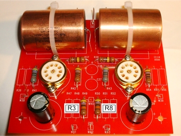
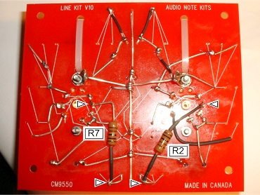
R3 and R8 are inserted next. One end connects to the ground bus while the other end is looped and inserted through the board to create terminals W41 and W43. Other component legs will be connected to this; hence creating a slight raised loop.
|
|
|
|
Here, we are working purely on the back of the board. One end of these resistors connects to pin 7 of the valve base. The other connects to the loop we made at W41/W43.
If you have the Level A kit then the analog board is now complete. However, if like myself you have the Level B kit then two more component pairs are required. For a Level B build, it may actually be more sensible to install R2 and R7 last of all because the I/V resistors and capacitors connect under these! |
|
|
|
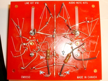
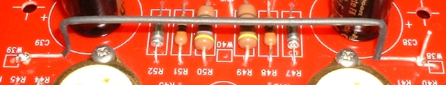
Now the I/V resistors are inserted. One end connects to the ground bus (routing under R2/R7) the and the other connects to the loop we made at W41/W43.
|
|
|
|
|
Finally the I/V capacitors are inserted. One end connects to the ground bus (routing under R2/R7) and the other connects to the loop we made at W41/W43.
|
|
The only thing left to do to finish off the analog board is to bridge between the two HT terminals W38 and W39 as they share the same HT line from the M2 power supply. I did this by using the last of the silver wire; bending it out of the way of any components and valves.
The analog board is now fully complete and ready to be placed in the chassis and wired to the M2 power supply board.
|
|